
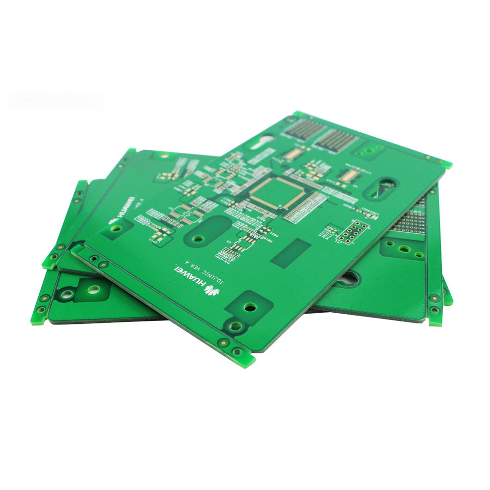

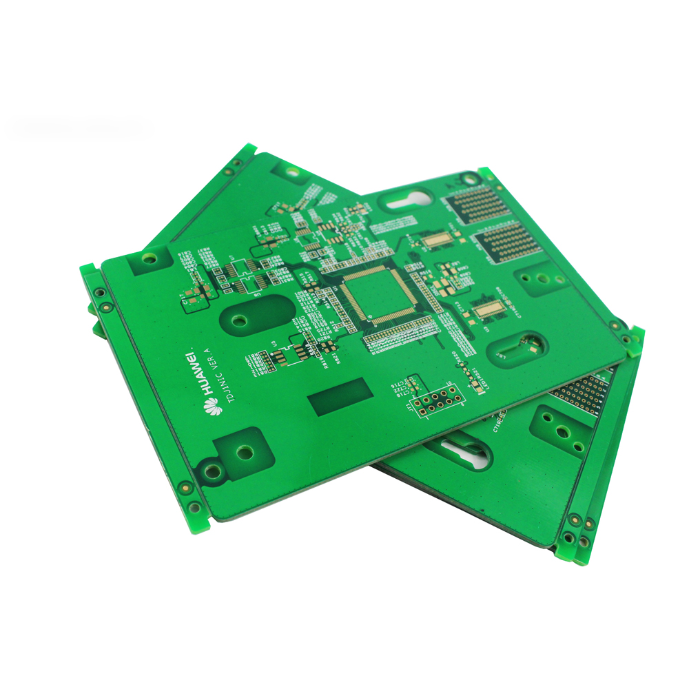
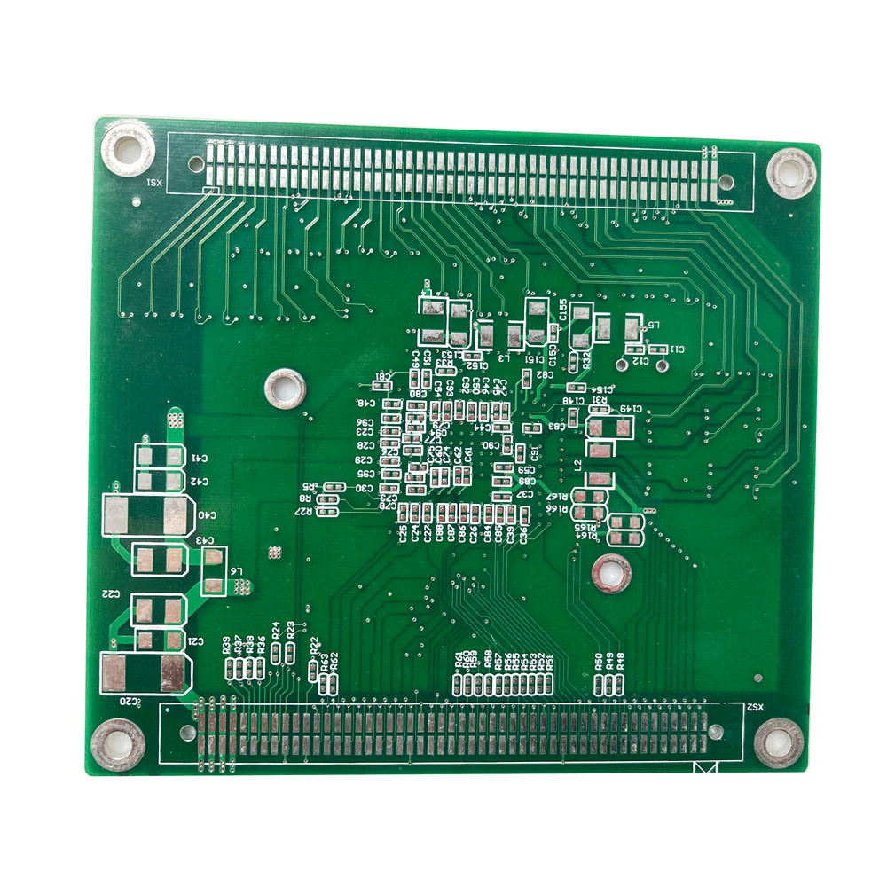
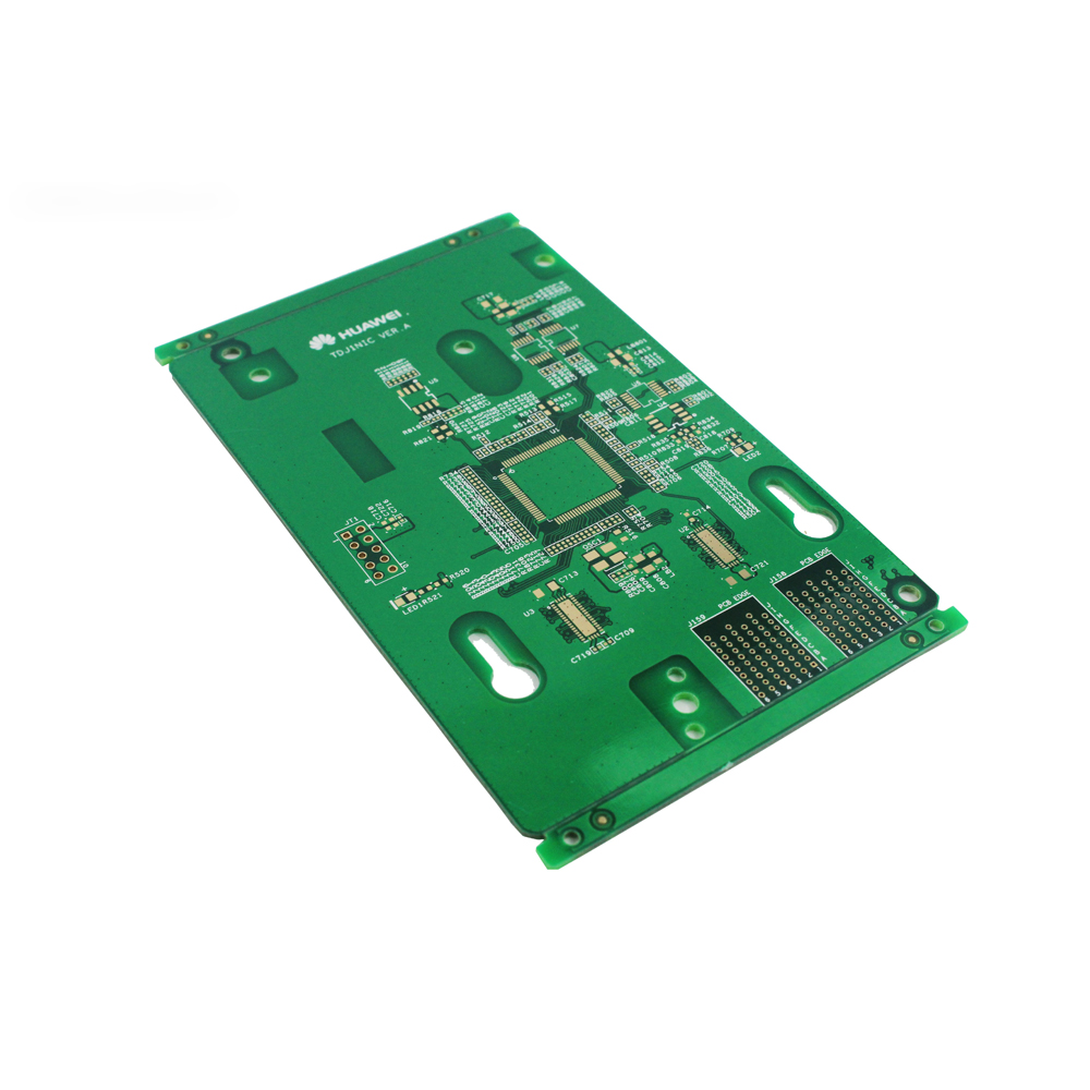

High Frequency PCBs
Multi-layer PCB Layout:
High frequency circuits are often highly integrated and with high wiring density. The use of multilayer board is both a necessary and an effective means to reduce interference. In PCB layout stage, a reasonable choice of a certain size and layers PCB, can make full use of an intermediary to set up the block, better nearby grounding, and effectively reduce the parasitic inductance and shorten the length of the transmission of signals, but also can greatly reduce the cross interference of signals etc., all of these methods are good for the reliability of the high frequency circuit. With the same material, the noise of four-layer board is 20dB lower than that of double-panel board. However, at the same time, there is also a problem, that is, the more layers of PCB boards have, the more complicated the manufacturing process would be, and the higher the unit cost would be, which requires that in the PCB layout, in addition to selecting appropriate layers of PCB, the reasonable components layout planning should be carried out and proper wiring rules should be adopted to complete the design.
1. The less alternating leads of the pins between the layers of high frequency circuits, the better.
This means that the less Via is used in connection, the better. A Via can bring about a distribution capacitance of about 0.5pF, reducing the number of Via can significantly increase the speed and reduce the possibility of data error.
2. The shorter the lead between the pins of high-frequency circuits is, the better it is.
The radiation intensity of the signal is directly proportional to the routing length of the signal line. The longer the high-frequency signal lead is, the more easily it can be coupled to its components. Therefore, for high frequency signal lines such as signal clock, crystal oscillator, DDR data, LVDS, USB and HDMI, the shorter the routing length is required, the better.
3. The less bend between the pins of high-frequency electronic devices, the better.
High frequency electrical wiring leads had better use full straight line. If a break over is required, a 45 degree broken line or arc break can be used. This requirement is only used to improve the bonding strength of copper foil in low-frequency circuits, while in high-frequency circuits, meeting this requirement can reduce the external emission and coupling of high-frequency signals.
4. Pay attention to the "crosstalk" introduced by the signal line parallel to close distance.
For high frequency circuit wiring, attention should be paid to the "crosstalk" introduced by the signal line parallel in a close distance. Crosstalk refers to the coupling phenomenon between signal lines without direct connection. Since high frequency signals are transmitted along the transmission line in the form of electromagnetic waves, the signal line will act as an antenna, and the energy of electromagnetic field will be emitted around the transmission line. The unwanted noise signals between signals due to the coupling of electromagnetic fields are called Crosstalk. The parameters of PCB plate layer, the spacing of signal lines, the electrical characteristics of driving and receiving terminals and the signal line connection mode all have certain influence on the crosstalk. Therefore, in order to reduce the crosstalk of high frequency signals, it is required to do the following as much as possible in the layout process.
(1) If there is a serious crosstalk between two lines, a ground line or ground plane can be inserted with, under the condition that the cabling space allows, it can play the role of isolation and reduce crosstalk.
(2) When the space around the signal line itself has time-varying electromagnetic fields, if the parallel distribution cannot be avoided, a large area of "ground" can be arranged on the opposite side of the parallel signal line to greatly reduce the interference.
(3) On the premise of sufficient wiring space, we can increase the space between adjacent signal lines and reduce the parallel length of signal lines. The clock line should be perpendicular to the key signal lines rather than parallel.
(4) If parallel lines in the same layer are almost unavoidable, they must be perpendicular to each other in the adjacent layers.
(5) In digital circuits, the usual clock signal is the edge changes fast signal, the external crosstalk is large. Therefore, in the design, it is advisable for the clock lines to be surrounded by the ground lines and digging more holes for the ground lines to reduce the distributed capacitance and thus reduce the crosstalk.
(6) The low voltage differential clock signal should be used as far as possible for the high frequency signal clock, and the integrity of the perforation should be paid attention to.
(7) The idle input is not to be suspended, but to be grounded or connected to a power supply, because the suspended line may be equivalent to the transmitting antenna, grounding can inhibit transmission.
5. High frequency digital signal ground line and analog signal ground line for isolation.
The analog ground line, digital ground line and so on connect to the common ground line to use high frequency choke magnetic bead connection or isolate directly and select the appropriate single point connection. High frequency digital signal of ground wire ground potential is not consistent, both directly there is often a voltage difference, and the high frequency digital signal ground wire is often contain very rich, the harmonic component of high frequency signal ground when connected directly to a digital signal and analog signal ground, the high frequency signal harmonic will through the way of the ground coupled to the analog signal interference. Therefore, in general, the ground line of high-frequency digital signal and the ground line of analog signal should be isolated, and the single point interconnection mode can be adopted in the appropriate location, or the high frequency choke magnetic bead interconnection mode can be adopted.
6. Increasing the high frequency decoupling capacitance of the power pins of IC block.
The power pins of each IC block add a high frequency demultiplexing capacitance nearby. Increasing the high frequency decoupling capacitance of the power pins of IC block, which can effectively inhibit the interference of high frequency harmonics on the power supply pin.
7. Avoid loops when wiring.
All kinds of high frequency signals should not form a loop when wiring. If it is unavoidable, the loop area should be as small as possible.
8. Good signal impedance matching must be ensured.
During the transmission process, when the impedance does not match, the signal will be reflected in the transmission channel, which will make the synthetic signal overshoot, causing the signal to fluctuate near the logical threshold. The basic method to eliminate reflection is to make the impedance of the transmission signal a good match. As the difference between the load impedance and the characteristic impedance of the transmission line is larger, the reflection is larger, so the characteristic impedance of the signal transmission line should be equal to the load and impedance as much as possible. At the same time, it should also be noted that the transmission line on the PCB cannot present sudden changes or corners, and keep the impedance of each point of the transmission line continuous as much as possible, otherwise reflection will occur between each segment of the transmission line. This requires the following wiring rules to be followed when conducting high-speed PCB wiring:
(1) LVDS wiring rules. The LVDS signal is required to make differential routing, with line width of 7mil and line distance of 6mil.
(2) USB wiring rules. USB signal is required for differential routing, line width is 10mil, line distance is 6mil, ground line and signal line spacing 6mil;
(3) HDMI wiring rules. HDMI signal differential routing is required, with line width of 10mil and line spacing of 6mil, each spacing between the two sets of HDM1 differential signals is more than 20mil.
(4) DDR wiring rules. DDR1 routing requires the signal not to go through the hole as far as possible. Signal line width is equal, and line and line are equidistant. Routing must meet the 2W principle to reduce crosstalk between signals.
In addition to the above mentioned design methods, engineers should try to avoid high-speed signal routing branches or tree stumps when designing PCB signal wiring. High frequency signal line is easy to generate large electromagnetic radiation when walking on the surface. If the high frequency signal line is wired between the power source and ground line, the radiation generated by absorbing the electromagnetic wave through the power source and the bottom layer will be greatly reduced. To sum up, high-frequency circuits are often highly integrated and with high wiring density. The use of multilayer boards is both a necessary and effective means to reduce interference. In PCB Layout stage, reasonable choice of a certain layer printed circuit board size, the middle tier can be fully used to set the shielding, better implement nearby ground, and effectively reduce the parasitic inductance and shorten the length of the transmission of signals, but also can greatly reduce the cross interference of signals etc., all of these methods are good for the reliability of the high frequency circuit.