
About Us


High Density Interconnect (HDI) PCB
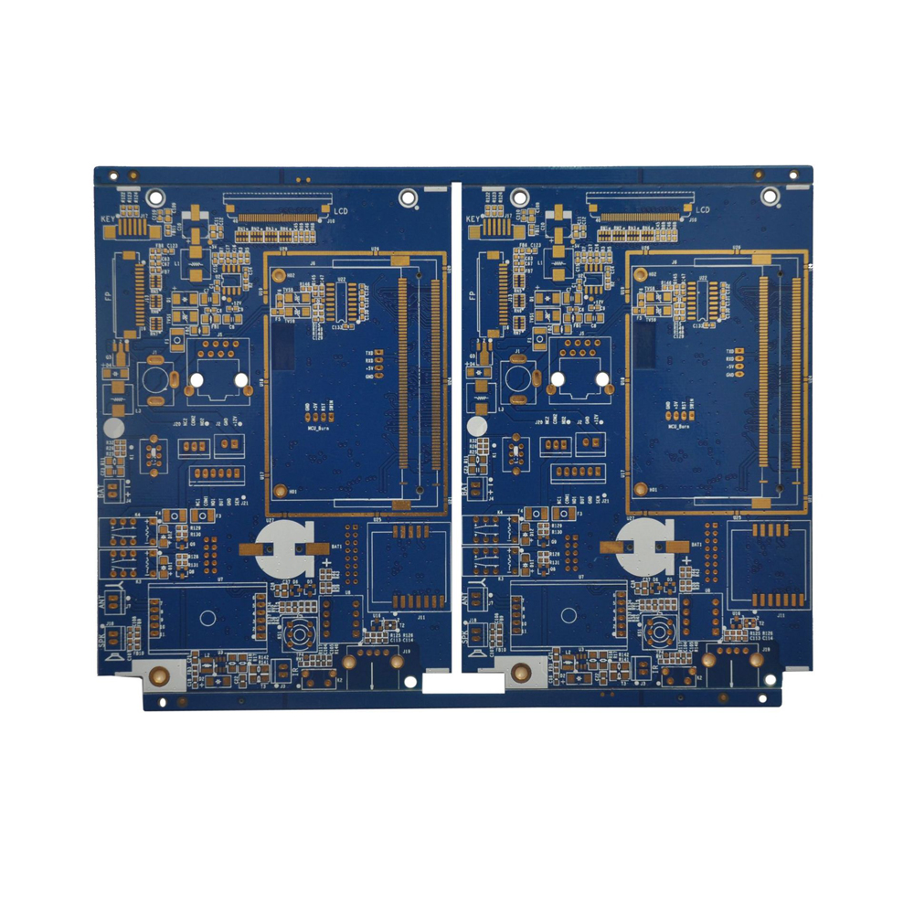
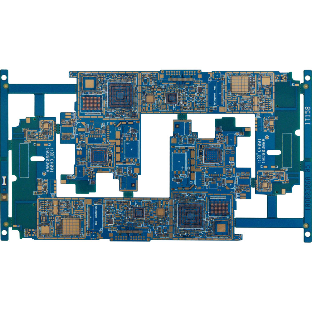
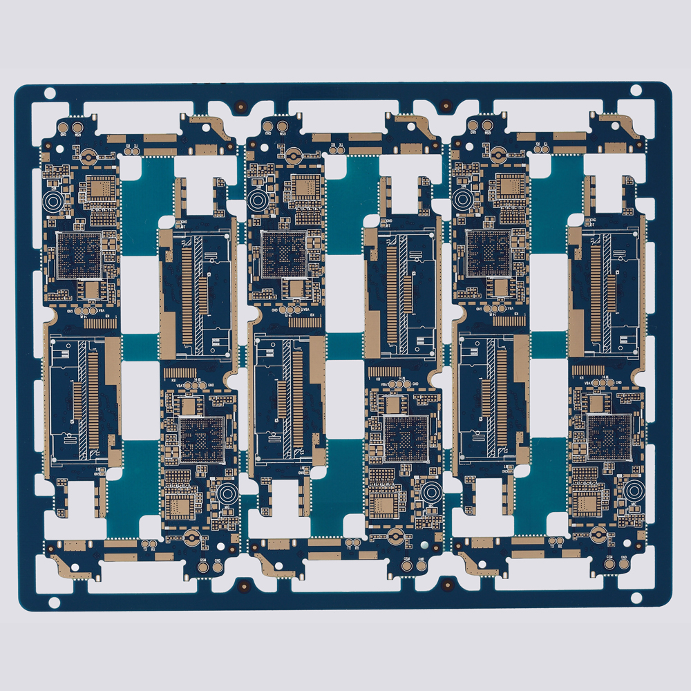
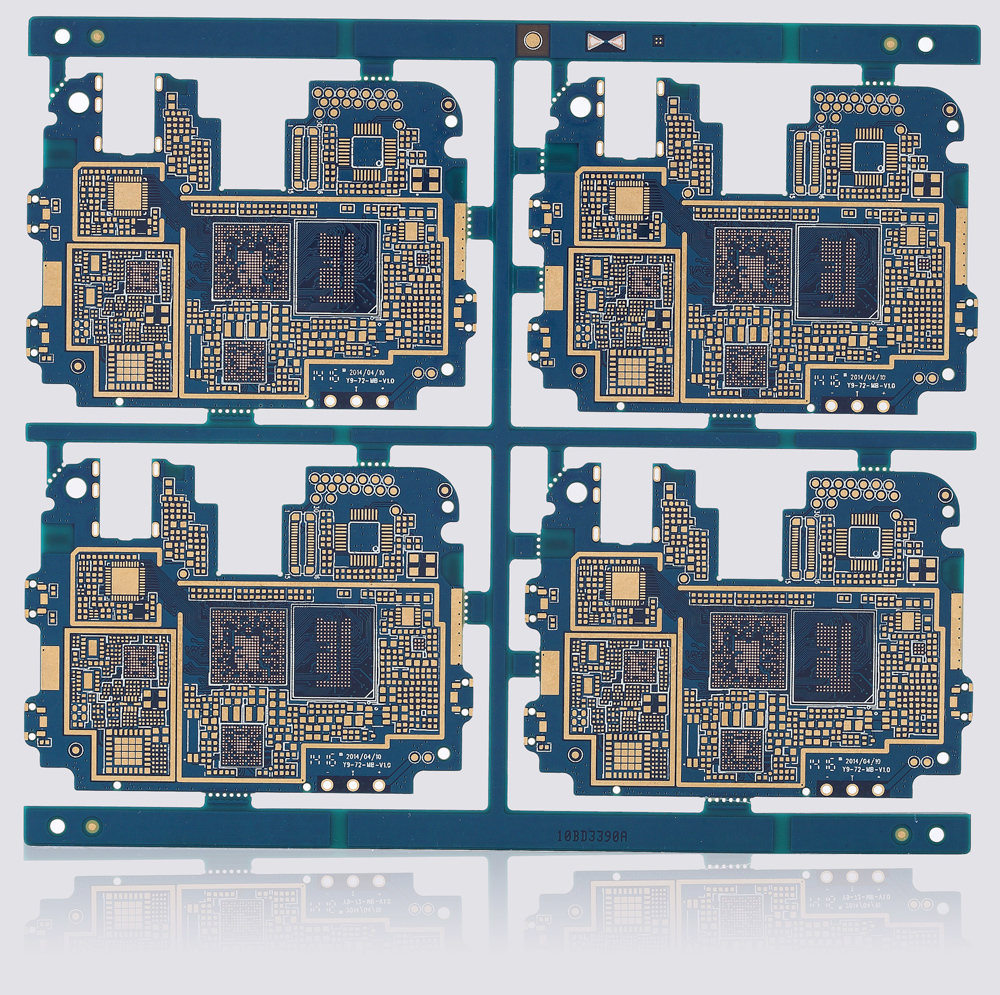
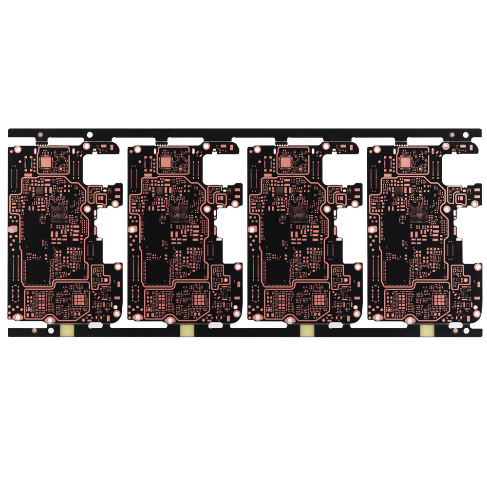
To meet the various needs of customers all over the world, Shanxu pcb not only provides common PCB fabrication and PCB assembly, but also High Density Interconnect (HDI) PCB turn-key electronics manufacturing services. The most manufacturing techniques for HDI PCB boards include blind & buried via, micro-via, epoxy resin or copper filled via, Controlled Impedance, fine lines in BGA pads, via in pad, etc. The HDI boards we manufactured refer to many fields like IoT, telecom electronic, smart control, industrial control and digital devices.
Description
Package Information
Inquiry
To meet the various needs of customers all over the world, Shanxu pcb not only provides common PCB fabrication and PCB assembly, but also High Density Interconnect (HDI) PCB turn-key electronics manufacturing services. The most manufacturing techniques for HDI PCB boards include blind & buried via, micro-via, epoxy resin or copper filled via, Controlled Impedance, fine lines in BGA pads, via in pad, etc. The HDI boards we manufactured refer to many fields like IoT, telecom electronic, smart control, industrial control and digital devices.
The capabilities for HDI PCB boards manufacturing
√ Blind & Buried via
√ Controlled Impedance
√ Epoxy Resin or Copper Filled Via
√ Fine Lines in BGA Pads
√ Via in Pad
√ Hybrid Laminate
| HDI PCB Capability | |||
| Category | Item | English | Metric |
| Laminates | Max. Number of Layers | 40 L | 40 L |
| Thickness of Thinnest 8 Layers HDI | 0.023" | 0.6 mm | |
| The Thinnest Core | 3 mil (no copper) | 0.075 mm (no copper) | |
| Finished Board Thickness Tolerance | ± 10% | ± 10% | |
| Trace | Min. Inner Layer Line Width | 2 mil | 0.05 mm |
| Min. Inner Layer Line Spacing | 2 mil | 0.05 mm | |
| Min. Outer Layer Line Width | 2 mil | 0.05 mm | |
| Min. Outer Layer Line Spacing | 2 mil | 0.05 mm | |
| Key Trace and Tolerance | 3 mil±0.6mil | 0.075 mm±15um | |
| Holes | Hole Position Tolerance | ± 3 mil | ± 0.075 mm |
| Hole Size Tolerance(PTH) | ± 3 mil | ± 0.075 mm | |
| Hole Size Tolerance(NPTH) | ± 2 mil | ± 0.05 mm | |
| Key HDI Process | HDI Layer | 3+N+3 | 3+N+3 |
| Controlled Impedance Tolerance | ± 8% | ± 8% | |
| Min. Solder Mask Bridge | 2.5 mil | 0.065 mm | |
| Min. Blind Hole Size | 4 mil | 0.1 mm | |
| PTH & Buried Hole | 6 mil | 0.15 mm | |
| Min. Pad with Via | 7 mil | 0.175 mm | |
| Min. BGA Pitch | 13.7 mil | 0.35 mm | |
| Min. BGA Pad | 8 mil | 0.2 mm | |
| Drill | Min. Mechanical Drill Hole Size | 6 mil | 0.15 mm |
| Min. Laser Drill Hole Size | 3 mil | 0.075 mm | |
| Aspect Ratio | 12:1 | 12:1 | |
| Gold Finger | Angle of Beveling | 15-45° | 15-45° |
| Angle of Beveling Tolerance | ± 5° | ± 5° | |
| Depth of Beveling | ≥ 4 mil | ≥ 0.1 | |
| Depth of BevelingTolerance | ± 3 mil | ± 0.075 mm | |
| Color of Solder Mask | Green | Matte Green | Light Green |
| Black | Matte Black | Red | |
| Yellow | White | Blue | |
| Color of Silk Screen | White | Black | Yellow |
| Green | Red | Blue | |
| Surface Finishing | HASL | HASL Lead Free | OSP |
| Immersion Gold (ENIG) | Gold Finger | Solf Gold | |